

Sequential Logic Blocks for Digital IC Design
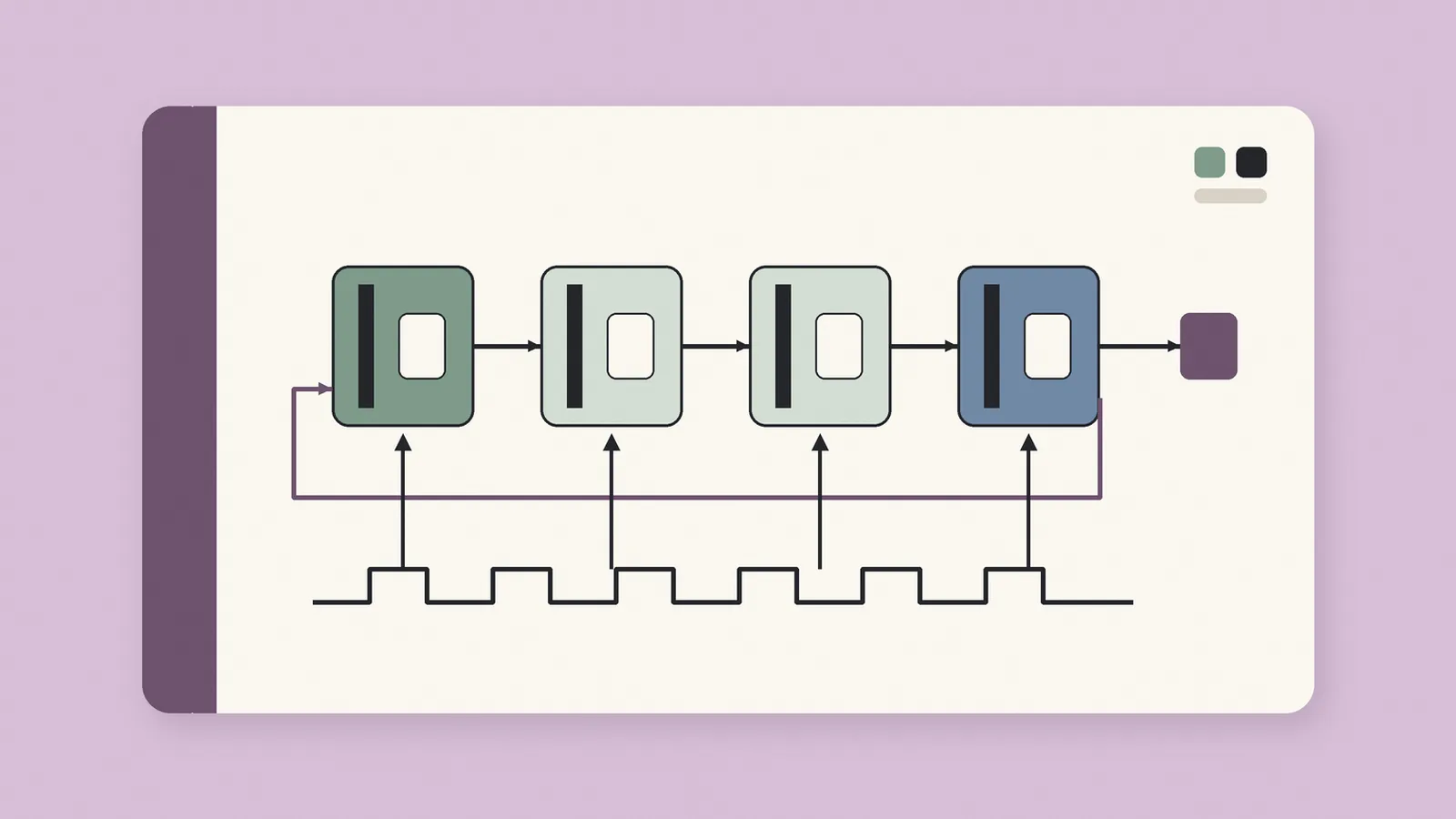
Sequential logic relies on latches, flip-flops, registers, counters, and FSMs to store state under clock control. Timing behavior, setup and hold limits, clock skew, metastability, and reset handling determine reliability, performance, and predictability in digital systems.
This resource includes
Description
Sequential logic provides the storage behavior required for digital systems to remember state, coordinate data movement, and perform controlled operations over time. Latches and flip-flops define the foundation of this behavior. A latch responds to a clock level and can remain transparent while enabled, allowing data to pass through during part of the clock cycle. A flip-flop samples data only at a clock edge, creating a sharper timing boundary and simpler reasoning about state changes. Timing behavior determines whether stored values are valid and reliable. Combinational logic between storage elements introduces delay, and each path must satisfy setup and hold requirements at the receiving element. Setup timing limits the maximum clock frequency because data must arrive early enough before sampling. Hold timing protects newly captured data from changing too soon after sampling. Violating these requirements can lead to incorrect data capture or metastability. Clock distribution strongly affects sequential design. The clock network has insertion delay, branch delay differences, skew, and jitter. These effects change the timing relationship between registers and reduce the effectiv...
This resource includes
Description
Sequential logic provides the storage behavior required for digital systems to remember state, coordinate data movement, and perform controlled operations over time. Latches and flip-flops define the foundation of this behavior. A latch responds to a clock level and can remain transparent while enabled, allowing data to pass through during part of the clock cycle. A flip-flop samples data only at a clock edge, creating a sharper timing boundary and simpler reasoning about state changes. Timing behavior determines whether stored values are valid and reliable. Combinational logic between storage elements introduces delay, and each path must satisfy setup and hold requirements at the receiving element. Setup timing limits the maximum clock frequency because data must arrive early enough before sampling. Hold timing protects newly captured data from changing too soon after sampling. Violating these requirements can lead to incorrect data capture or metastability. Clock distribution strongly affects sequential design. The clock network has insertion delay, branch delay differences, skew, and jitter. These effects change the timing relationship between registers and reduce the effectiv...
Recommended

EDA Academy is a practical learning platform for engineers in the VLSI and semiconductor industry. We offer structured courses, technical resources, and career-focused training across all major areas of chip design and verification — from Verilog to Physical Design, from fundamentals to advanced topics. Learn at your own pace, explore member-exclusive content, or join as an instructor to share your expertise. Lear...
