

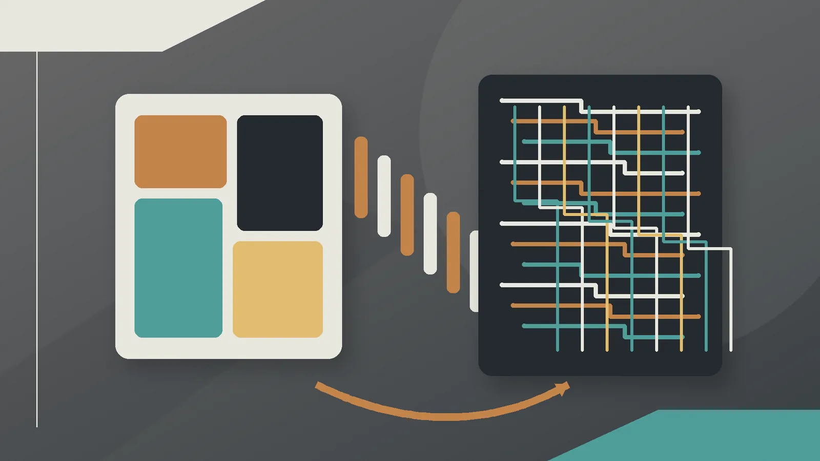

From Floorplanning to Routing Closure
Transform logical hardware into manufacturable silicon layout through floorplanning, placement, timing closure, routing, and physical verification. Key topics include block planning, macro placement, I/O organization, clocking effects, routing congestion, utilization control, and verification-driven implementation quality.
This resource includes
Description
Physical design turns logical circuit intent into a geometric silicon layout that can satisfy timing, routing, power, and manufacturing requirements. The process begins with implementation planning, where the design is organized into physical regions and prepared for downstream optimization. A top-level netlist provides the logical connectivity, while physical constraints define die size, block area, I/O organization, power resources, and early implementation limits. Floorplanning establishes the first major physical structure of the chip. It defines die dimensions, allocates area for soft blocks, places or reserves space for macros, organizes I/O locations, and prepares power structures. Block placement, module organization, utilization control, and routing-resource planning are handled at this stage to reduce downstream risk. Flightlines and connectivity views help reveal communication intensity between blocks, allowing highly connected regions to be placed closer together and reducing unnecessary wire length. Placement converts the floorplan into legal cell locations. Sites and rows define where cells may be placed, while library information determines the legal row type for e...
This resource includes
Description
Physical design turns logical circuit intent into a geometric silicon layout that can satisfy timing, routing, power, and manufacturing requirements. The process begins with implementation planning, where the design is organized into physical regions and prepared for downstream optimization. A top-level netlist provides the logical connectivity, while physical constraints define die size, block area, I/O organization, power resources, and early implementation limits. Floorplanning establishes the first major physical structure of the chip. It defines die dimensions, allocates area for soft blocks, places or reserves space for macros, organizes I/O locations, and prepares power structures. Block placement, module organization, utilization control, and routing-resource planning are handled at this stage to reduce downstream risk. Flightlines and connectivity views help reveal communication intensity between blocks, allowing highly connected regions to be placed closer together and reducing unnecessary wire length. Placement converts the floorplan into legal cell locations. Sites and rows define where cells may be placed, while library information determines the legal row type for e...
Recommended

EDA Academy is a practical learning platform for engineers in the VLSI and semiconductor industry. We offer structured courses, technical resources, and career-focused training across all major areas of chip design and verification — from Verilog to Physical Design, from fundamentals to advanced topics. Learn at your own pace, explore member-exclusive content, or join as an instructor to share your expertise. Lear...
