

Clock Gating Techniques for Low-Power Design
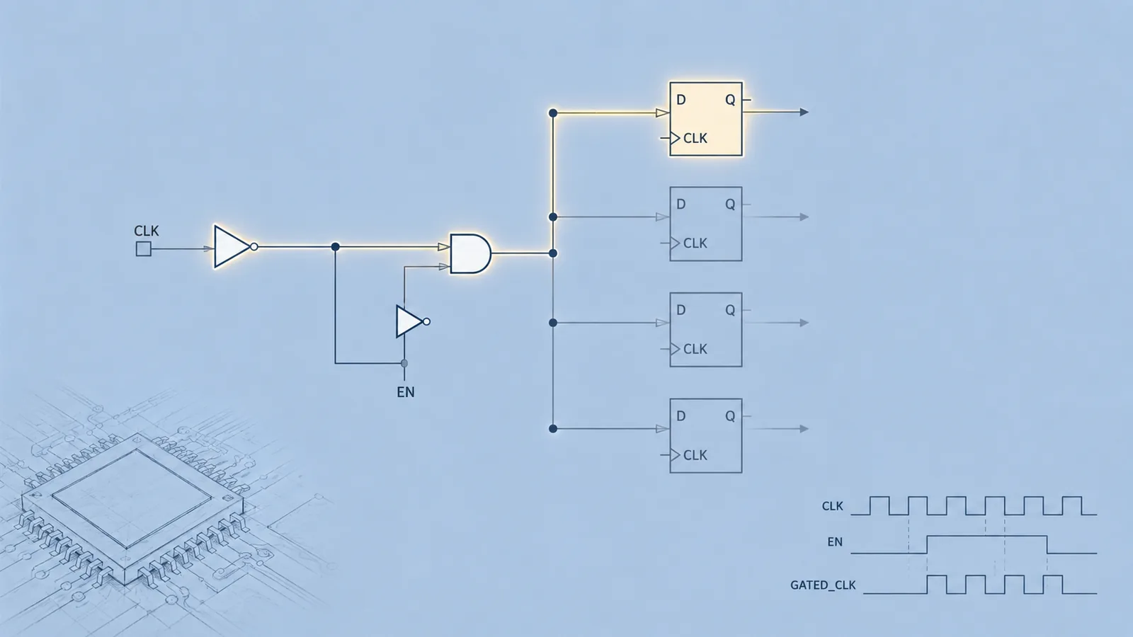
Clock gating reduces CMOS dynamic power by limiting unnecessary clock switching in inactive sequential logic. Explains RTL power strategies, gated-clock structures, synthesis insertion, multi-stage optimization, physical implementation concerns, and equivalence checking for functionally safe low-power design.
This resource includes
Description
CMOS power consumption is strongly influenced by switching activity, and the clock network is one of the most active structures in a synchronous digital design. Every unnecessary clock edge can charge and discharge capacitance across clock buffers, interconnect, register clock pins, and internal sequential circuitry. Clock gating targets this activity directly by disabling clock propagation when registers do not need to update, reducing dynamic power while preserving the intended functional behavior. RTL provides an effective entry point for identifying inactive logic. Enable-controlled registers, shared control signals, and idle data paths can be analyzed before physical implementation. Operand isolation can reduce switching around unused operators, while clock gating can remove unnecessary clock activity from sequential logic. When registers share the same enable condition, synthesis can group them and insert a shared clock-gating function, reducing repeated activity across larger portions of the design. Practical clock gating requires more than inserting a gate on a clock path. Gating cells, user-defined modules, and logic-based gates must be handled with attention to enable s...
This resource includes
Description
CMOS power consumption is strongly influenced by switching activity, and the clock network is one of the most active structures in a synchronous digital design. Every unnecessary clock edge can charge and discharge capacitance across clock buffers, interconnect, register clock pins, and internal sequential circuitry. Clock gating targets this activity directly by disabling clock propagation when registers do not need to update, reducing dynamic power while preserving the intended functional behavior. RTL provides an effective entry point for identifying inactive logic. Enable-controlled registers, shared control signals, and idle data paths can be analyzed before physical implementation. Operand isolation can reduce switching around unused operators, while clock gating can remove unnecessary clock activity from sequential logic. When registers share the same enable condition, synthesis can group them and insert a shared clock-gating function, reducing repeated activity across larger portions of the design. Practical clock gating requires more than inserting a gate on a clock path. Gating cells, user-defined modules, and logic-based gates must be handled with attention to enable s...
Recommended

EDA Academy is a practical learning platform for engineers in the VLSI and semiconductor industry. We offer structured courses, technical resources, and career-focused training across all major areas of chip design and verification — from Verilog to Physical Design, from fundamentals to advanced topics. Learn at your own pace, explore member-exclusive content, or join as an instructor to share your expertise. Lear...
