


Systematic Dynamic Power Reduction in CMOS Design
Analyze CMOS power dissipation mechanisms and reduce dynamic power through voltage scaling, switching activity control, operand isolation, clock gating, synthesis optimization, and physical implementation techniques across the digital IC design flow.
This resource includes
Description
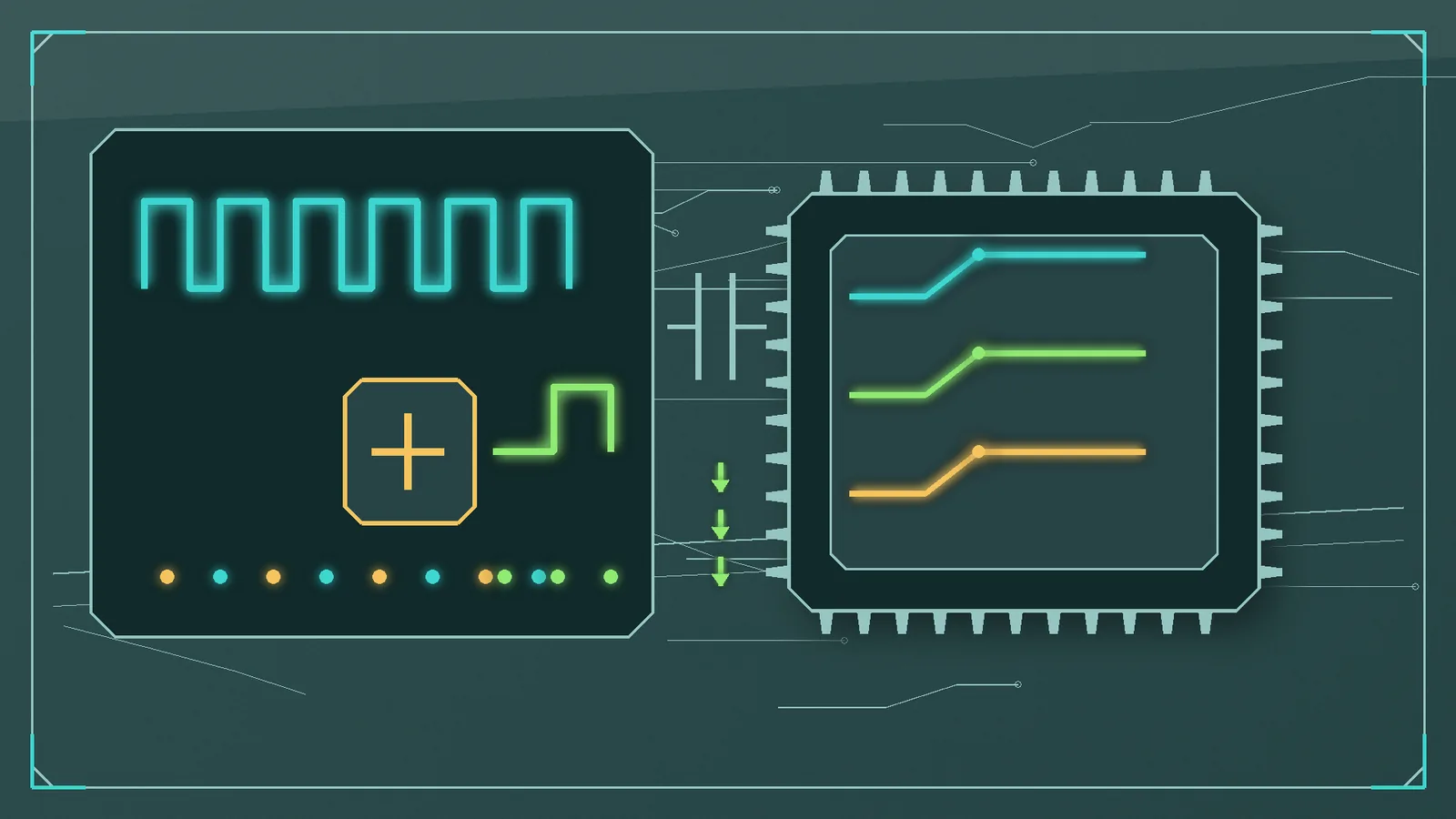
Dynamic power is one of the most important constraints in digital CMOS design. It comes primarily from charging and discharging capacitive loads during signal transitions, with additional contribution from short-circuit current during switching. Its magnitude is driven by switching activity, effective capacitance, supply voltage, and clock frequency. These factors provide a clear engineering model for identifying where power is consumed and how meaningful reductions can be achieved. Technology scaling has made power optimization more difficult and more important. Lower supply voltages reduce switching energy, but lower threshold voltages increase leakage. Smaller transistors improve density, while interconnect capacitance and clock distribution remain major sources of dynamic consumption. The result is a design environment where power must be considered from architecture through physical implementation, rather than treated as a late-stage cleanup task. Architecture-level decisions define the largest power-saving opportunities. Voltage-domain planning, workload partitioning, performance targets, memory organization, parallelism, and clocking strategy all shape active power before ...
This resource includes
Description
Dynamic power is one of the most important constraints in digital CMOS design. It comes primarily from charging and discharging capacitive loads during signal transitions, with additional contribution from short-circuit current during switching. Its magnitude is driven by switching activity, effective capacitance, supply voltage, and clock frequency. These factors provide a clear engineering model for identifying where power is consumed and how meaningful reductions can be achieved. Technology scaling has made power optimization more difficult and more important. Lower supply voltages reduce switching energy, but lower threshold voltages increase leakage. Smaller transistors improve density, while interconnect capacitance and clock distribution remain major sources of dynamic consumption. The result is a design environment where power must be considered from architecture through physical implementation, rather than treated as a late-stage cleanup task. Architecture-level decisions define the largest power-saving opportunities. Voltage-domain planning, workload partitioning, performance targets, memory organization, parallelism, and clocking strategy all shape active power before ...
Recommended

EDA Academy is a practical learning platform for engineers in the VLSI and semiconductor industry. We offer structured courses, technical resources, and career-focused training across all major areas of chip design and verification — from Verilog to Physical Design, from fundamentals to advanced topics. Learn at your own pace, explore member-exclusive content, or join as an instructor to share your expertise. Lear...
