

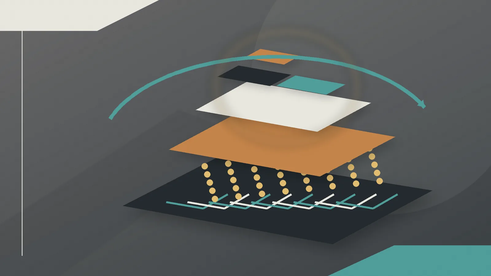

IC Package Design and Co-Optimization Flow
IC package design transforms die interfaces into manufacturable, electrically reliable components through substrate definition, I/O planning, netlist optimization, constraint-driven routing, wire bond modeling, flip chip integration, and IC–package–PCB co-optimization for high-density silicon systems.
This resource includes
Description
IC package design defines the physical, electrical, thermal, and mechanical bridge between silicon and the electronic system. It converts die-level connectivity into package-level structures that can be assembled onto a printed circuit board while preserving signal quality, power integrity, thermal performance, and long-term reliability. As transistor density increases, package I/O demand grows quickly, forcing package architectures to move from simple peripheral pin arrangements toward dense area-array interconnects, advanced substrates, and multi-die integration strategies. Package efficiency provides a practical way to evaluate how effectively active silicon area is mapped into board-level footprint. Silicon scaling can reduce die size, but package dimensions are limited by I/O pitch, escape routing, power delivery, assembly tolerances, and manufacturing constraints. Advanced integration methods such as die stacking, multi-chip modules, chiplet architectures, and interposer-based packages allow total active silicon area to increase without proportional growth in board attachment area. This changes the package from a protective enclosure into an active integration platform. Die...
This resource includes
Description
IC package design defines the physical, electrical, thermal, and mechanical bridge between silicon and the electronic system. It converts die-level connectivity into package-level structures that can be assembled onto a printed circuit board while preserving signal quality, power integrity, thermal performance, and long-term reliability. As transistor density increases, package I/O demand grows quickly, forcing package architectures to move from simple peripheral pin arrangements toward dense area-array interconnects, advanced substrates, and multi-die integration strategies. Package efficiency provides a practical way to evaluate how effectively active silicon area is mapped into board-level footprint. Silicon scaling can reduce die size, but package dimensions are limited by I/O pitch, escape routing, power delivery, assembly tolerances, and manufacturing constraints. Advanced integration methods such as die stacking, multi-chip modules, chiplet architectures, and interposer-based packages allow total active silicon area to increase without proportional growth in board attachment area. This changes the package from a protective enclosure into an active integration platform. Die...
Recommended

EDA Academy is a practical learning platform for engineers in the VLSI and semiconductor industry. We offer structured courses, technical resources, and career-focused training across all major areas of chip design and verification — from Verilog to Physical Design, from fundamentals to advanced topics. Learn at your own pace, explore member-exclusive content, or join as an instructor to share your expertise. Lear...
