

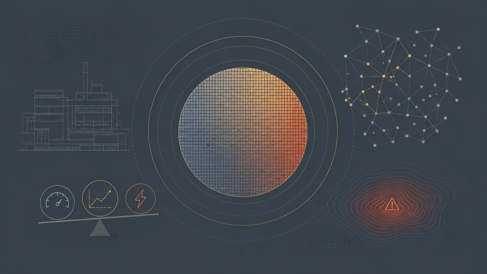

The Scale of Digital IC Design
Explore why modern digital IC design is a high-risk, high-reward engineering challenge, covering transistor scale, process nodes, wafer economics, fabs, tapeout pressure, PPA tradeoffs, thermal limits, verification complexity, and the continuing need for human creativity.
This resource includes
Description
Modern digital IC development combines semiconductor physics, large-scale engineering, manufacturing economics, verification strategy, and strict market timing. A small silicon die can contain tens of billions of transistors, hundreds of billions of interconnects, and many process layers. These structures are manufactured on wafers inside fabs that cost billions of dollars, operate continuously, and require rigid scheduling discipline. The result is an engineering environment where physical scale, financial scale, and schedule pressure are inseparable. The technical foundation starts with the physical structure of ICs: silicon regions form transistors, metal layers provide interconnect, and vias connect layers into a dense three-dimensional system. Process-node names, transistor density, Moore’s Law, wafer output, and fab economics explain why semiconductor design is both difficult and financially attractive. A successful chip can ship in enormous volume, but a failed tapeout can consume tens or hundreds of millions of dollars and destroy a market opportunity. Design optimization centers on power, performance, and area. Area affects wafer cost and die count. Performance depends o...
This resource includes
Description
Modern digital IC development combines semiconductor physics, large-scale engineering, manufacturing economics, verification strategy, and strict market timing. A small silicon die can contain tens of billions of transistors, hundreds of billions of interconnects, and many process layers. These structures are manufactured on wafers inside fabs that cost billions of dollars, operate continuously, and require rigid scheduling discipline. The result is an engineering environment where physical scale, financial scale, and schedule pressure are inseparable. The technical foundation starts with the physical structure of ICs: silicon regions form transistors, metal layers provide interconnect, and vias connect layers into a dense three-dimensional system. Process-node names, transistor density, Moore’s Law, wafer output, and fab economics explain why semiconductor design is both difficult and financially attractive. A successful chip can ship in enormous volume, but a failed tapeout can consume tens or hundreds of millions of dollars and destroy a market opportunity. Design optimization centers on power, performance, and area. Area affects wafer cost and die count. Performance depends o...
Recommended

EDA Academy is a practical learning platform for engineers in the VLSI and semiconductor industry. We offer structured courses, technical resources, and career-focused training across all major areas of chip design and verification — from Verilog to Physical Design, from fundamentals to advanced topics. Learn at your own pace, explore member-exclusive content, or join as an instructor to share your expertise. Lear...
