

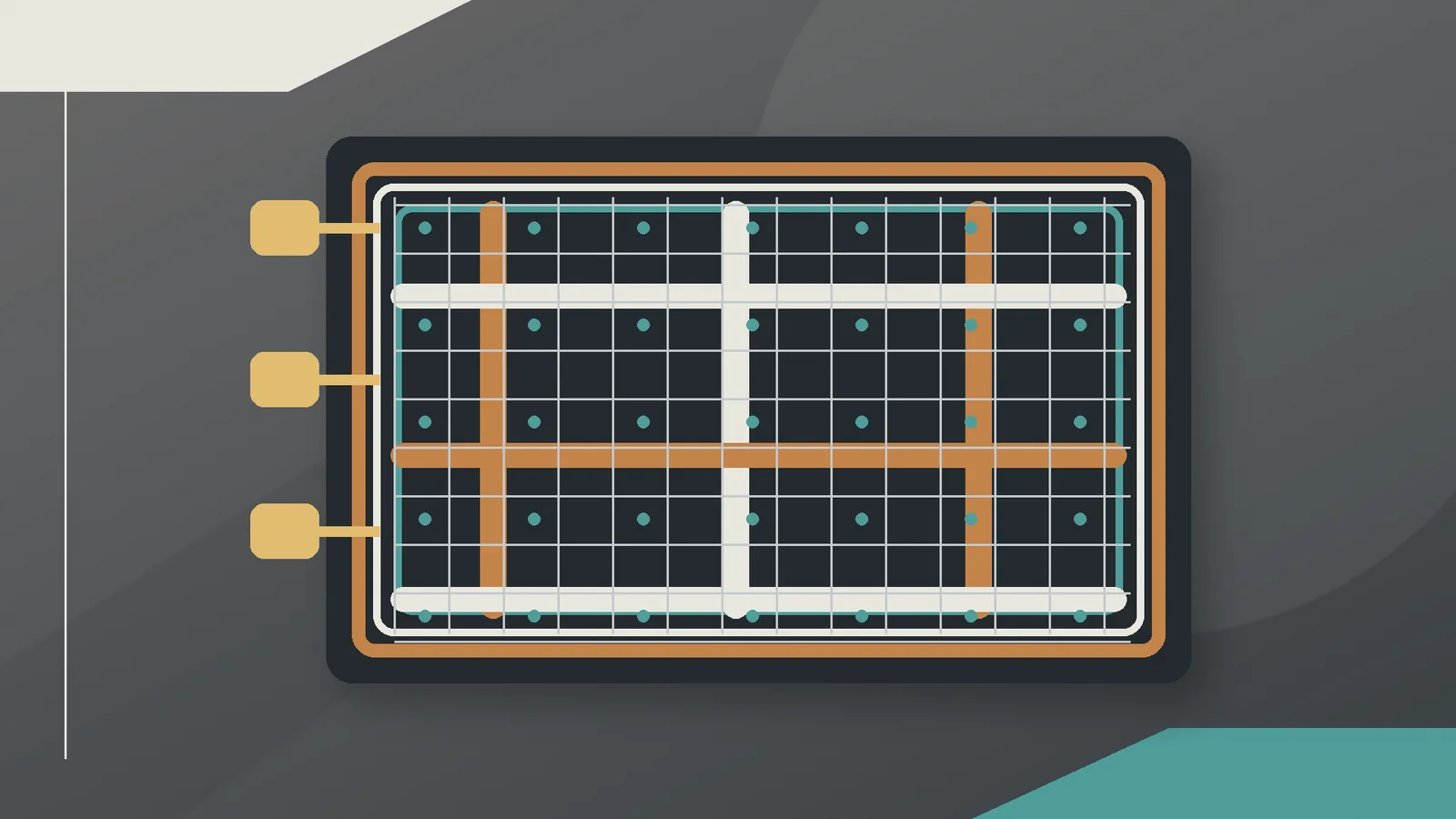

Power Planning for Reliable Chip Delivery
Power planning defines reliable power and ground delivery for digital ICs through rings, stripes, rails, meshes, vias, and routing structures, while managing IR drop, electromigration, power consumption, routing resources, and multi-voltage power domains.
This resource includes
Description
Power planning is a core physical design activity that defines how supply and ground networks are built across a digital integrated circuit. It determines how current enters the chip, how it reaches macros and standard cells, and how stable voltage is maintained under real switching conditions. A well-structured power delivery network supports timing closure, functional correctness, manufacturability, and reliability by giving every part of the design a strong electrical path to VDD and VSS. The main technical focus is power integrity. Current flowing through resistive metal creates IR drop, reducing the actual voltage available to logic cells. Excessive voltage loss can damage timing margin and cause failures during high activity. High current density also creates electromigration risk, gradually weakening metal wires and vias over time. These issues require systematic control through wire sizing, metal layer selection, via capacity, mesh density, and early rail analysis. The physical network is built from several connected structures. Power pads bring supply into the chip. Core rings and block rings distribute current around major regions. Power stripes and meshes spread curren...
This resource includes
Description
Power planning is a core physical design activity that defines how supply and ground networks are built across a digital integrated circuit. It determines how current enters the chip, how it reaches macros and standard cells, and how stable voltage is maintained under real switching conditions. A well-structured power delivery network supports timing closure, functional correctness, manufacturability, and reliability by giving every part of the design a strong electrical path to VDD and VSS. The main technical focus is power integrity. Current flowing through resistive metal creates IR drop, reducing the actual voltage available to logic cells. Excessive voltage loss can damage timing margin and cause failures during high activity. High current density also creates electromigration risk, gradually weakening metal wires and vias over time. These issues require systematic control through wire sizing, metal layer selection, via capacity, mesh density, and early rail analysis. The physical network is built from several connected structures. Power pads bring supply into the chip. Core rings and block rings distribute current around major regions. Power stripes and meshes spread curren...
Recommended

EDA Academy is a practical learning platform for engineers in the VLSI and semiconductor industry. We offer structured courses, technical resources, and career-focused training across all major areas of chip design and verification — from Verilog to Physical Design, from fundamentals to advanced topics. Learn at your own pace, explore member-exclusive content, or join as an instructor to share your expertise. Lear...
